| I. Research Purpose Active-matrix organic light-emitting diode (AMOLED) displays have become the mainstream monitors owing to the advantages of high contrast, high color saturation, wide viewing angle, and flexibility. However, the conventional 2T1C circuit causes the nonuniformity of the display image due to the variations of the threshold voltage of the thin-film transistor, OLED degradation, and I-R drop. Thus, we propose relevant research results for the above-mentioned issues and different applications. |
|
|
|
Conventional n-type and p-type 2T1C AMOLED pixel circuit. |
|
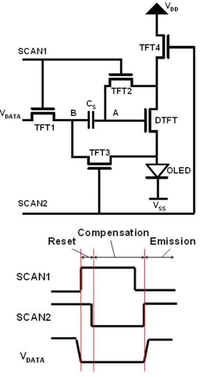
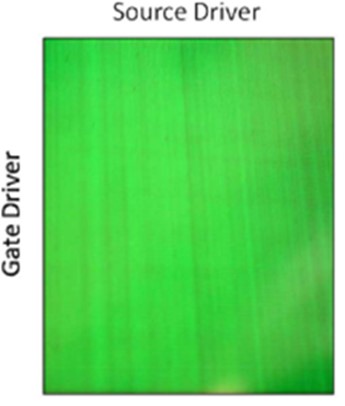
| II. Research Results 1. OLED degradation Our laboratory proposed the concept of compensation for OLED degradation in the world firstly and designed the relevant compensating circuit. This circuit can not only compensate the variations of the threshold voltage of the driving TFT but also use the feedback structure for increasing the driving current to compensate the nonuniform image brightness as OLED degrades, extending the lifetime of the AMOLED panel and realizing the high image quality display. Compared with the conventional 2T1C pixel circuit, the proposed circuit can achieve high uniform image of the AMOLED display panel. |
||
(a) |
(b) |
(c) |
(a) Proposed compensating pixel circuit for OLED degradation. Comparison of image uniformity achieved with (b) conventional 2T1C panel and (c) proposed 5T1C panel. |
||
|---|---|---|
|
2. High resolution
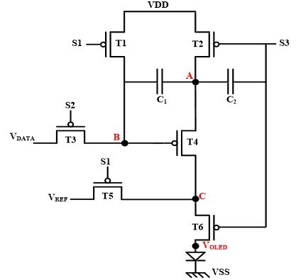
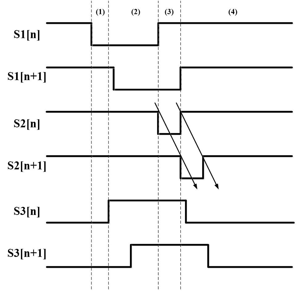
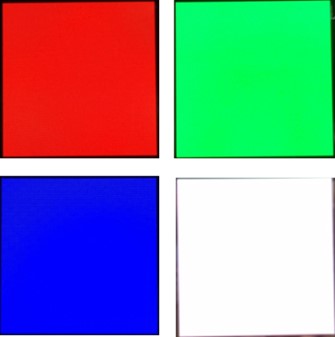
Our laboratory proposed a compensating pixel circuit with the parallel driving scheme, published in IEEE Journal of Solid-State Circuits. For the issue of insufficient compensation time in high resolution, the proposed circuit does not use the reference voltage of the data line in the compensating period. Thus, the compensation time is not restricted by the resolution. The data input and compensating periods are independent, so the pixel circuits of different rows can be simultaneously compensated to prolong the compensation time and improve the compensation effect of the circuit. When the compensation time is extended, the relative error rate can be effectively suppressed at low in all gray levels, proving that prolonging the compensation time can effectively improve the uniformity of the driving current. The photograph of fabricated panel also indicates the proposed circuit can effectively improve the uniformity of display image and be applied to the high resolution display. |
|||
(a) |
(b) |
||
(c) |
(d) |
||
(a) Proposed compensating pixel circuit with parallel driving scheme. (b) Timing diagram. |
|||
|---|---|---|---|
|
3. Low frame rate
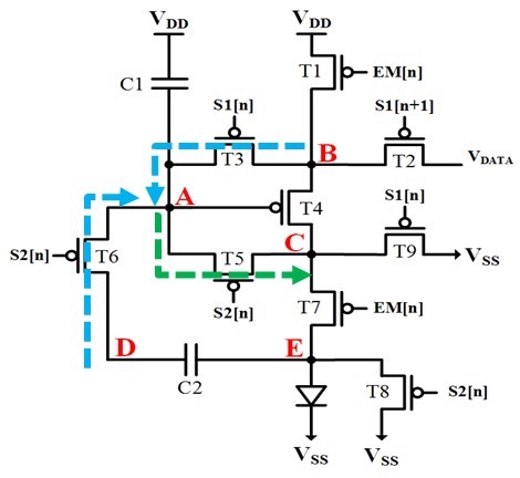
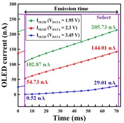
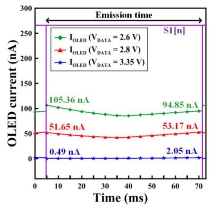
Since smartwatches need to operate at a low frame rate, the LTPS process is widely used in small—sized displays. However, the larger leakage currents make the gate voltage of the driving TFT vary and change the driving currents after a long period, affecting the uniformity of image. Our lab proposed a new leakage-prevention pixel circuit that can suppress the distortion of the driving voltage at the gate node of the driving TFT in the long emission period. Thus, the uniformity of the driving current can be effectively improved. Simulation results show that the proposed circuit used a leakage-prevention structure to compensate for leakage current of switching TFTs, enhancing the feasibility of the proposed circuit for use in the low frame rate smartwatch. |
||
(a) |
(b) |
(c) |
(a) Proposed leakage-prevention pixel circuit. Comparison of driving currents with (b) conventional pixel circuit and (c) proposed pixel circuit. |
||
|---|---|---|


