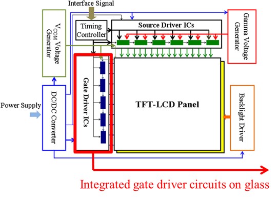
| I. Research Purpose The gate driver circuit (GOA) incorporates thin-film transistors integrated on glass substrates. It does not require external integrated circuits (ICs), and that can improve the reliability of the display panel system to realize low-cost, mechanically reliable displays. Thus, the gate driver circuit has become the mainstream display technology to meet the different requirements of displays, such as in-cell touch panels, low power consumption, narrow bezel, and high resolution. |
|
|
|
| II. Research Results 1. In-cell touch panel Our laboratory proposed a bidirectional gate driver circuit that applies the recharging and time-division driving methods for use in LCD panels with in-cell touch technology, published in IEEE Transactions on Industrial Electronics. This circuit can prevent the effect of the display-to-touch crosstalk and insufficient report rate, and simultaneously reduce the shift of the threshold voltage of a-Si:H thin-film transistors under long-term operation . The measurement results show that the proposed circuit can successfully realize the function of bidirectional transmission, and generate the continuous output waveforms after the touch sensing period. |
||

|

|
|
Proposed bidirectional gate driver circuit for in-cell touch panel and output waveforms. |
||
|
2. High resolution
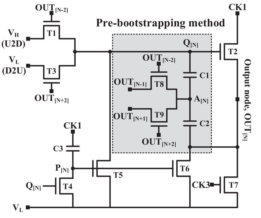
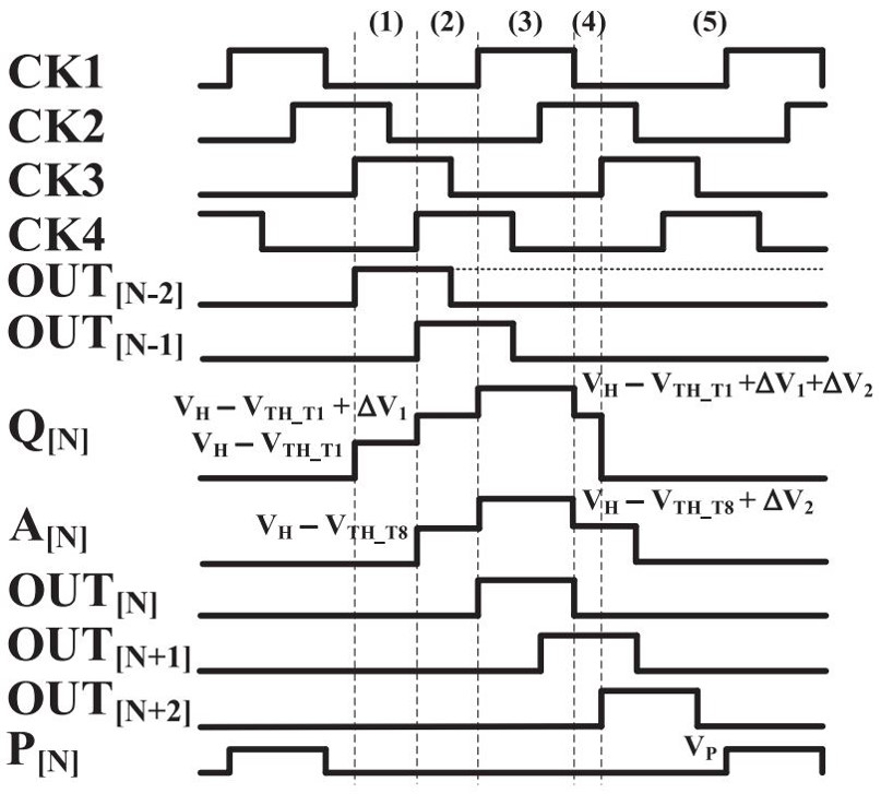
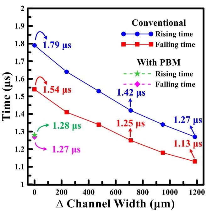
Our laboratory proposed a bidirectional gate driver circuit that uses pre-bootstrapping method to improve the driving capability of the a-Si:H TFT for high resolution display panels, published in IEEE Transactions on Industrial Electronics. The pre-bootstrapping method utilizes the capacitive coupling effect to bootstrap the gate voltage of the driving TFT twice to improve the insufficient field-effect mobility of the a-Si:H TFT without the need to enlarge the driving TFT. |
|||
(a) |
(b) |
||
(c) |
(d) |
||
(a) Proposed bidirectional gate driver circuit with pre-bootstrapping method. |
|||

|
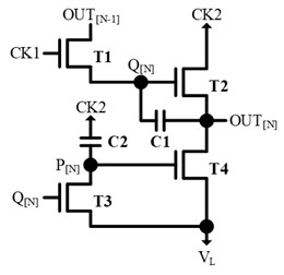
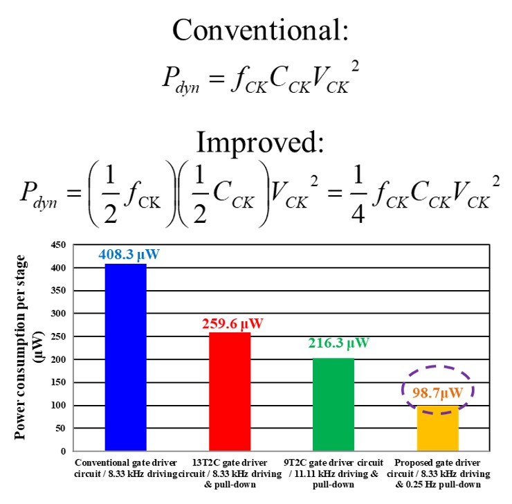
3. Low power consumption
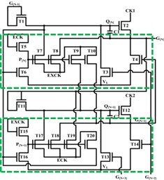
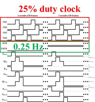
Our laboratory proposed a new low-power gate driver circuit that uses negative gate-to-source voltage for recovering the threshold voltage shifts of a-Si:H TFTs. Four clock signals (Ck1, CK2, CK3 and CK4) and two additional clock signals (ECK and EXCK) are used to improve the power consumption by reducing the frequency of the driving signal. Moreover, the synchronously controlled pull-down scheme subsequently reduces the number of TFTs to simplify the structure, and the low-frequency pull-down structure reduces the consumed power, achieving the effect of the low power consumption. |
||
|
|
|
Proposed low-power gate driver circuit, timing diagram, and comparison of power consumption with other gate driver circuits. |
||
|
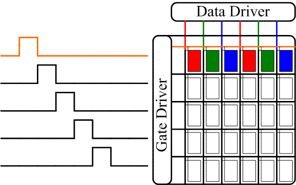
4. Narrow bezel
Our laboratory proposed a simplified gate driver circuit. With overlapping clock signals, the input TFT can charge and discharge the gate voltage of the driving TFT, and periodically restrain the clock-feedthrough effect after generating the gate pulse. Furthermore, the driving TFT can charge and discharge the output node, so no other large TFT is required to discharge the output node, realizing a simplified circuit. Moreover, the simulation results show that the proposed circuit can successfully generate continuous output waveforms, verifying the functionality of the circuit. Thus, this circuit is favorable for high resolution and narrow bezel displays. |
||
(a) |
(b) |
(c) |
(a) Proposed simplified gate driver circuit, system diagram, and layout of single-stage circuit. |
||